ISI utilizes its expertise to effectively provide space-efficient solutions and high-performance circuit integration that optimize the electrical and mechanical properties of systems. ISI has demonstrated consistent success in designing and manufacturing modules with bare dies.
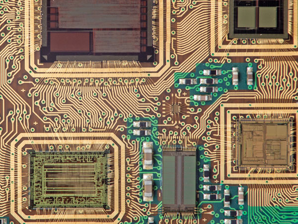
ISI’s Next-Level Integration packaging blends high-density packaging with advanced interconnect capabilities to promptly afford miniaturized solutions. These packaging techniques include:
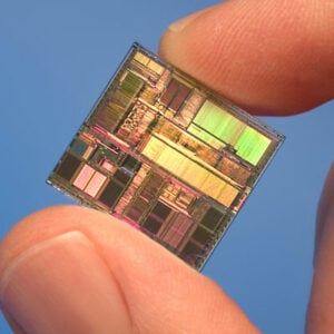
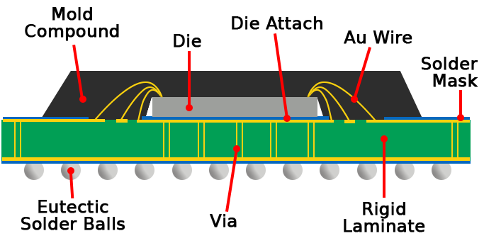
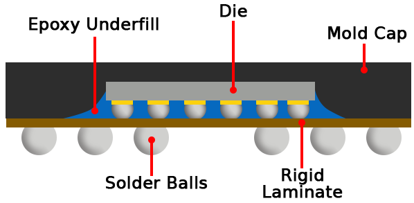
Once produced, bare die can be assembled by attaching it to a substrate or “packaged” through different processes. ISI has qualified a variety of stacked bare die techniques. These processes are available for use with standard die and do not require custom die or through-silicon vias (TSV). Below are the various die-stacking methods offered for bare die assembly.


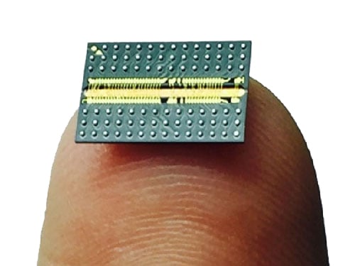
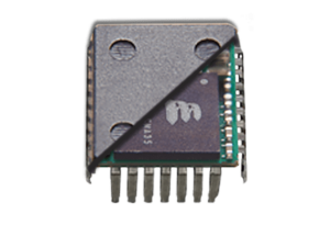
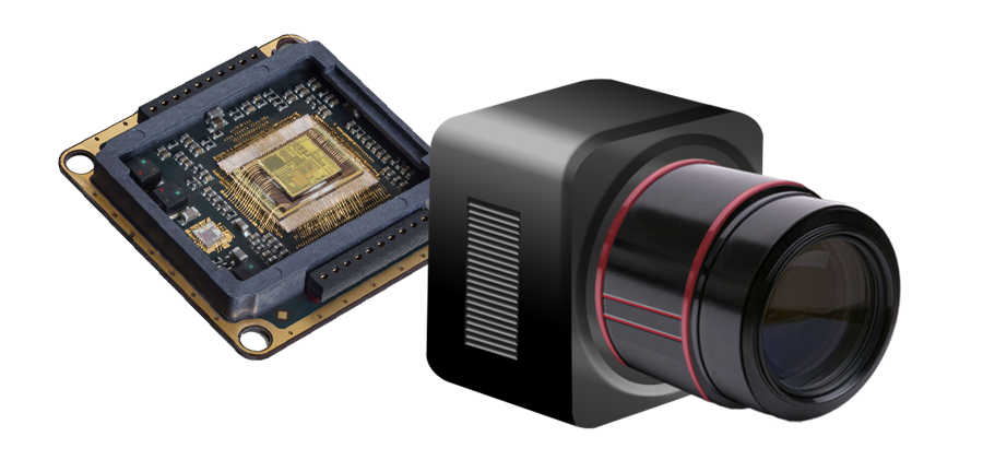
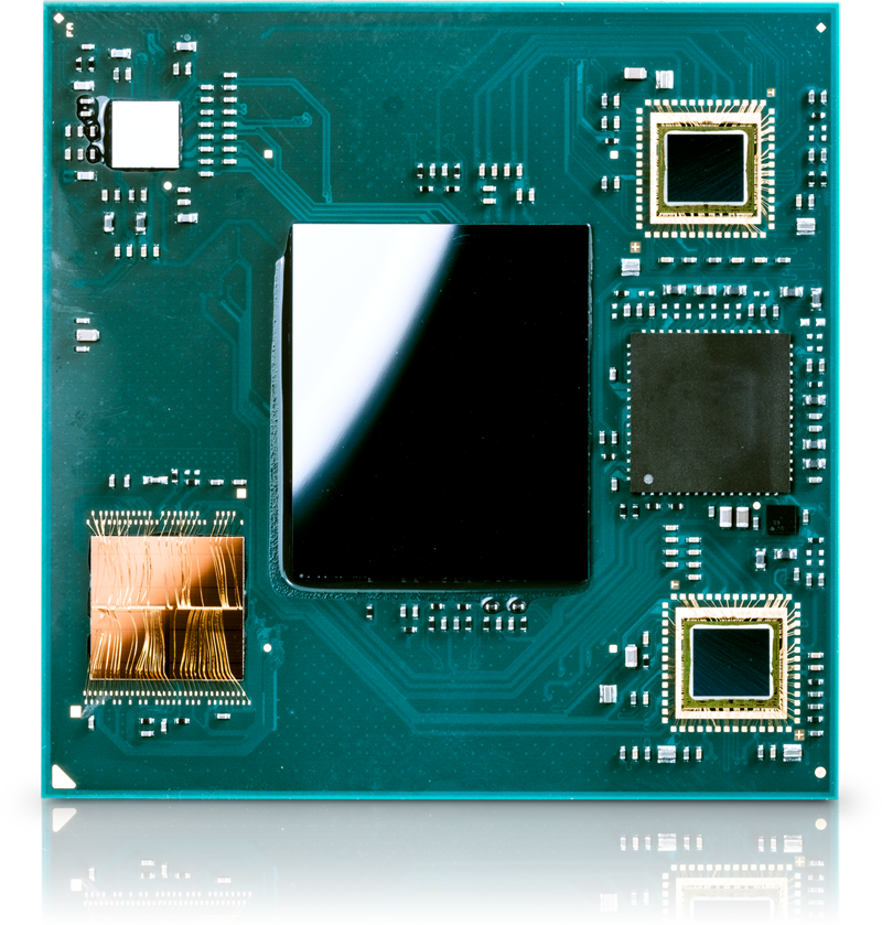
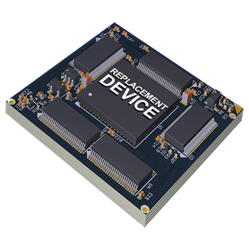
Ultra-dense, SWaP-optimized microelectronic assemblies.
Survive harsh environments;
Temperature cycle, shock, and vibration.
Integration of sensors with microelectronic modules.
Multi-component modules in standard IC form factor
(BGA, QFP, etc.).
Replace obsolete ICs with a form/fit/function equivalent module.
Your message will go to our in-house technical sales team. We typically get back within one business day.